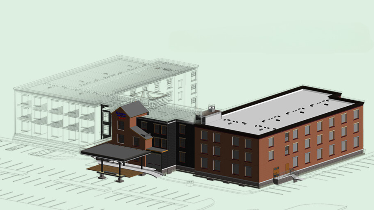
In the world of architecture, engineering, and construction, there are few facilities as intricate and crucial as semiconductor fabrication plants, commonly referred to as "fabs". These are the powerhouses behind our modern digital age, producing the tiny chips that drive almost every piece of electronic equipment we use. Given the complexity and sensitivity of these facilities, the use of Building Information Modeling (BIM) in their design and construction is not just beneficial – it's essential. Dive into this deep dive on why BIM is reshaping the future of semiconductor fabs.
Understanding the Inner World of a Semiconductor Fab
Imagine stepping into a space where even a single speck of dust could disrupt the production of hundreds of microchips. That’s the reality in a semiconductor fab. Here’s a breakdown of its labyrinthine design:
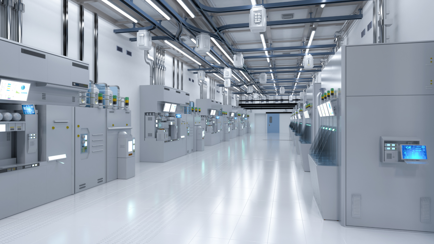
1. Cleanroom Areas:
Cleanroom Area
This is the heart of the fab. Picture a vast, sterile space where technicians in white suits move between large pieces of machinery. Every breath of air is filtered, with contaminants kept to an absolute minimum to protect delicate semiconductor wafers.
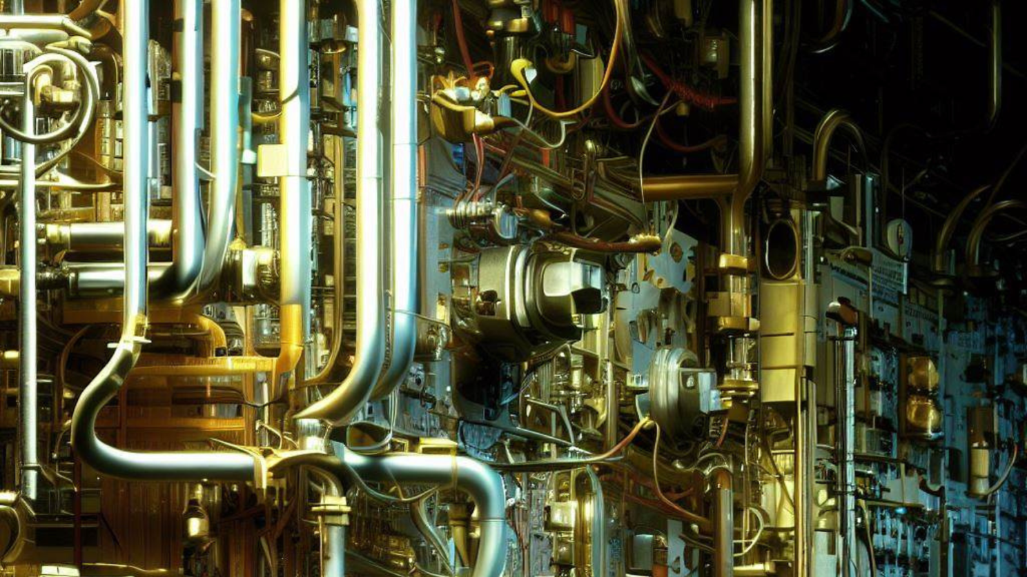
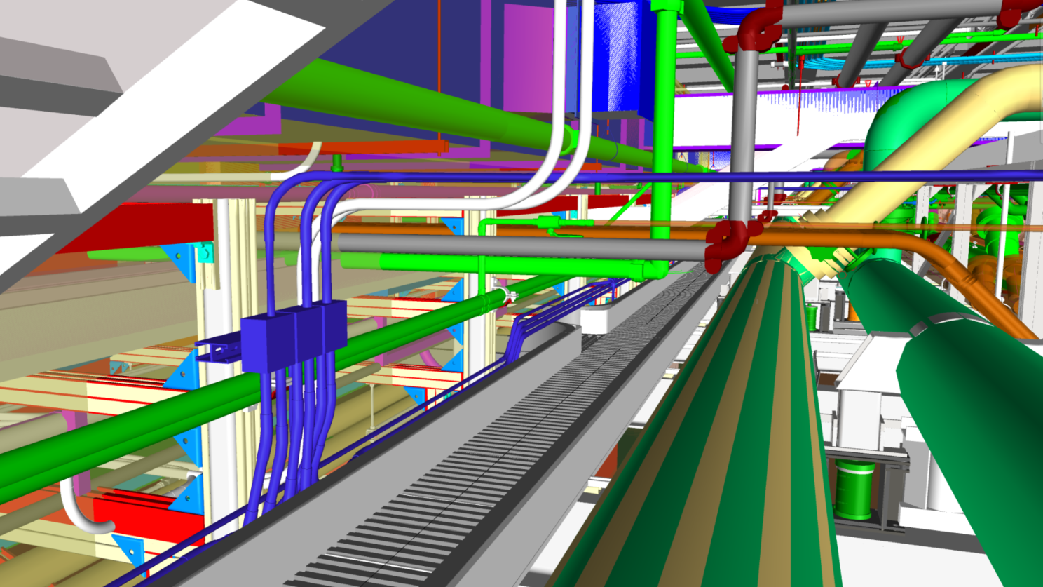
2. Subfab Areas:
subfab area
Like the engine room of a ship, the subfab area, located below the cleanroom, is a jungle of pipes, tanks, and equipment. It supports every process happening above.
3. Utilities and Corridors:
Utilities and Corridors
Winding through the fab are countless corridors carrying utilities—HVAC systems, chemical delivery lines, ultra-pure water systems, and waste management infrastructure.
4. Tool Hook-up:
Tool Hook-up
The lifeblood of the fab, these are the connections that provide individual manufacturing tools with power, gases, chemicals, and other essential utilities.
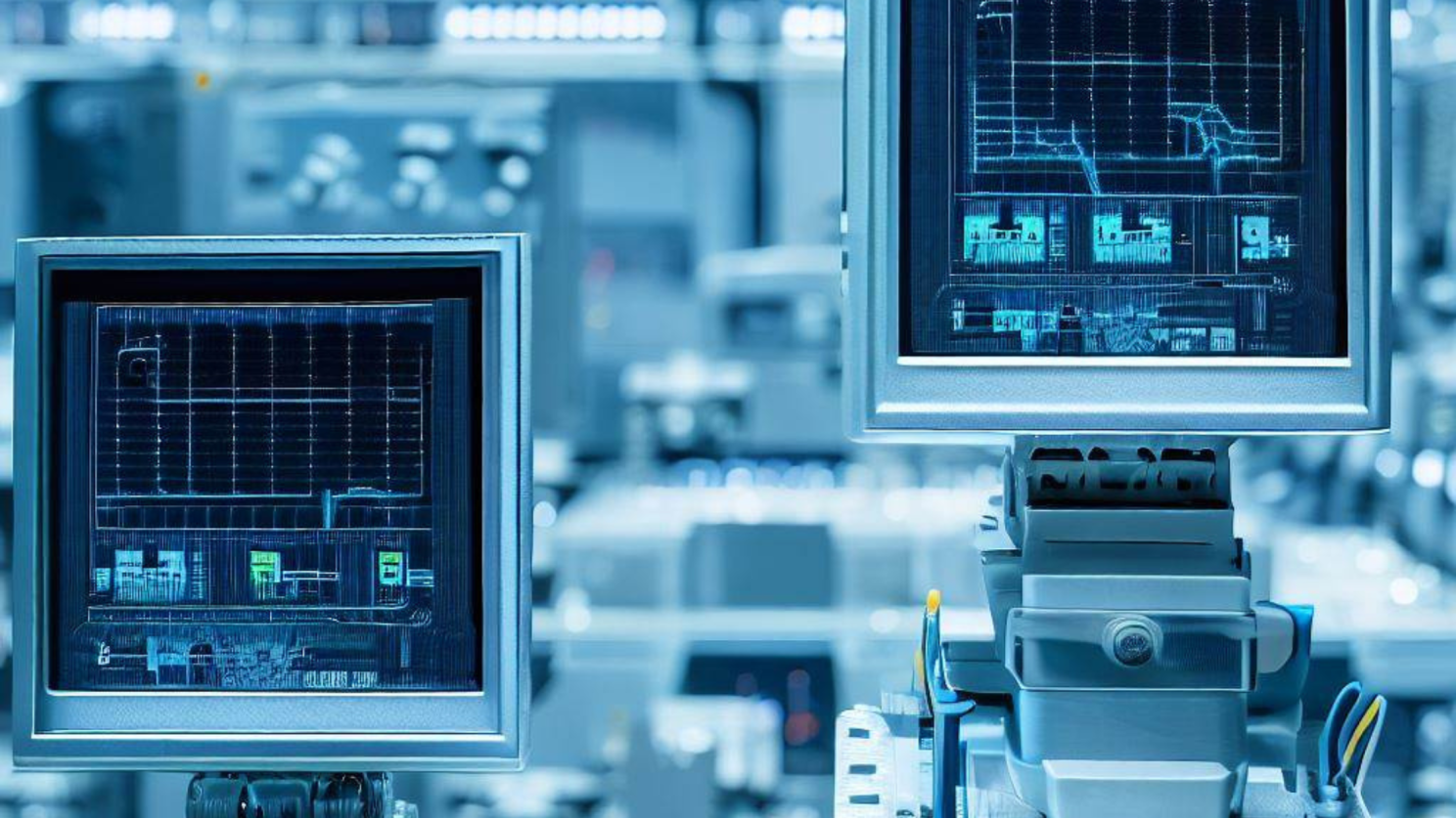
5. Facility Monitoring Systems:
Facility Monitoring Systems
These silent watchdogs keep an eye on parameters like temperature, humidity, and air quality, ensuring optimum conditions for semiconductor production.
6. Support Spaces:
Support Spaces
Beyond the high-tech manufacturing areas, fabs also feature office spaces, conference rooms, storage, and other ancillary areas.
Why BIM is a Game-Changer for Semiconductor Fabs
BIM goes beyond traditional 2D or 3D modeling; it's a holistic 3D design tool that also integrates time and cost. Its importance for fabs is multifold:
Spatial Coordination:
Spatial Coordination
With BIM, potential spatial conflicts between various systems can be identified in the design phase itself. This is invaluable in a fab, where even a minor oversight can have massive implications.
Time and Cost Integration:
Time and Cost Integration
Imagine visualizing the entire construction timeline or getting real-time cost estimates as design changes are made. This 4D and 5D integration ensures that fabs are not just designed efficiently but are also built on time and within budget.
Collaboration:
Collaboration
Multiple stakeholders from architects to engineers, from HVAC specialists to cleanroom experts, can work together on a unified BIM model. This promotes consistency, reduces errors, and improves efficiency.
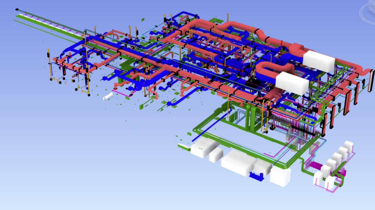
The Magic of Laser Scanning
Laser Scanning
BIM isn’t just about designing new fabs. Laser scanning technology allows existing facilities to be captured in minute detail. Once scanned, this data can be integrated into a BIM model—a process known as creating an "as-built BIM model." Benefits?
Design Verification:
Design Verification
Comparing the laser-scanned as-built model with the original BIM model can highlight inconsistencies. In fabs, where precision is paramount, this step is crucial.
Future Enhancements:
source: vectorworks
An as-built BIM model serves as a blueprint for future renovations or expansions.
Engaging with the Future
Imagine a scenario where a pipe needs replacing in a fab. Instead of poring over countless 2D drawings, a technician equipped with Augmented Reality (AR) glasses, powered by the BIM model, can be guided directly to the problem area, with every utility and potential obstacle mapped out in real-time.
Or consider energy modeling. Fabs are energy-hungry. A BIM model, when integrated with energy modeling tools, can predict and optimize a fab's energy consumption.
BIM model
In Conclusion: Why BIM Matters
At the crossroads of precision, technology, and design, BIM stands out as a beacon for the future of complex infrastructures like semiconductor fabs. As we continue to push the boundaries of microchip technology and demand more from our digital devices, the environments in which these chips are produced must keep pace. BIM, with its multi-dimensional approach and holistic integration of design, construction, and operation, ensures that semiconductor fabs are ready for the future's challenges.
Get in touch with Desapex to know how we can co-create such models and help your business grow.
BIM for Beginners' is designed to give you the essential knowledge and skills you need to succeed in the dynamic world of BIM engineering. This course opens doors to a rewarding career path in the construction industry.
Basics of BIM
Fundamentals of AutoCAD 2D and 3D
Fundamentals of Revit Architecture and Interference check
Thank you! Your submission has been received!
Oops! Something went wrong while submitting the form.
BIM for Beginners' is designed to give you the essential knowledge and skills you need to succeed in the dynamic world of BIM engineering. This course opens doors to a rewarding career path in the construction industry.
An amazing new feature you will love
Incredible, groundbreaking feature
Something that just blows your mind
Thank you! Your submission has been received!
Oops! Something went wrong while submitting the form.


.png)


